Sony and TSMC Plan Joint Venture for Image Sensors
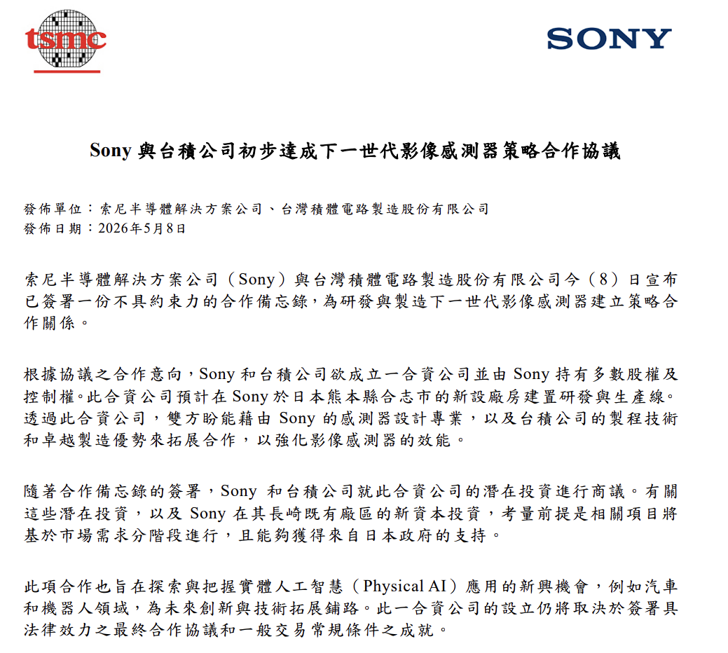
Sony Semiconductor Solutions (Sony) and TSMC announced on May 8th here, that the two parties have signed a non-binding memorandum of understanding to establish a strategic cooperative relationship focusing on the research and development and manufacturing of next-generation image sensors. According to current plans, they propose to establish a joint venture with Sony holding the majority stake and control.
The joint venture is expected to be located in Sony's new factory in Kpal, Kumamoto Prefecture, Japan, to undertake the research and development and production line construction of the next-generation image sensors. Sony provides sensor design capabilities, TSMC provides process technology and manufacturing capabilities, and the common goal is to improve the performance of image sensors and extend the cooperation to broader application scenarios.
The announcement specifically mentioned that the two parties hope to explore new opportunities in physical artificial intelligence applications. The automotive and robotics sectors are new opportunities both parties want to explore, which means that image sensors may move from traditional imaging components into machine perception and automation systems. The cooperation is still at the intention stage.
市场有风险,内容仅供研究参考,不构成投资建议。